Remotely Accessible Instruments for Nanotechnology (RAIN) Network
What is RAIN?
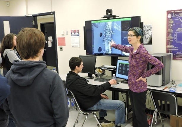
The Remotely Accessible Instruments for Nanotechnology (RAIN) Network allows students to access and control state-of-the-art characterization tools remotely, thus bringing the wonders of the nanoscale directly into their classrooms or home computers. Students control the tools over the internet in real-time and with the assistance of an experienced engineer through video conferencing software. Participating RAIN sites have characterization tools with cutting edge resolution far beyond that visible to the naked eye.
This network of remotely accessible scientific equipment lowers the barrier-to-entry and enables instructors to deliver authentic and relevant educational activities for students interested in learning about nanotechnology and other STEM fields. RAIN Network providers aim to increase nano-literacy and inspire the next generation STEM workforce (technicians, technologists, engineers, educators, and scientists) by engaging them in their day-to-day classrooms with live-stream connections to experts and tools in labs at institutions where cutting-edge research is being performed.
Activities have included “show-and-tell” outreach sessions, professional development workshops, program recruitment, student projects, and interactive in-class laboratories, allowing the students in the classroom to operate the featured equipment. Coordinators at each facility help advise educators on the best options to use RAIN most effectively for their courses and learning objectives. RAIN is an excellent example of educational institutions coming together to share their facilities, tools, and expertise with their local communities, who most often do not have the resources to attain and sustain these types of very expensive equipment.
A survey of students who have participated in RAIN sessions found a majority reported RAIN sessions as more engaging than traditional textbooks. Another study found RAIN sessions increased interest in science among underrepresented students who previously showed no passion for obtaining science degrees.
The RAIN Network was established as part of the National Science Foundation (NSF) Advanced Technological Education (ATE)-funded Nanotechnology Applications and Career Knowledge (NACK) Resource Center, located in the Center for Nanotechnology Education and Utilization (CNEU) at Penn State University.
back to top ↑
Remote Access Session
Explore
• The list of tools and associated videos to determine what will work best for your needs.
• The list of guides provided below or set up your own with your provider’s assistance.
• The Additional Resources below to learn more about nanotechnology.
Request
Contact a specific partner directly by clicking on the “more” link below their name.
OR
Fill out the Request Form. Tell us your:
• Learning objectives
• Preferred dates/times
• Desired tool(s) or preferred provider
Prepare
• Set up your computer. You need a webcam, microphone, speakers, mouse with scroll wheel, and projector or large display.
• Set up a test session ensure everything works as expected
• Choose your samples. You can use your own or the provider’s in-house samples.
Feedback
Instructor Survey – tell us about your experience requesting, testing, and running remote access.
Student Survey – share this survey with your students. We want to know if they enjoyed the experience and found it valuable.
back to top ↑
Available Equipment
Remote Hands-on Control
Atomic Force Microscope (AFM)
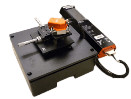
The atomic force microscope (AFM) is one of about two dozen types of scanned-proximity probe microscopes. All of these microscopes work by measuring a local property – such as height, optical absorption, or magnetism – with a probe or “tip” placed very close to the sample. The small probe-sample separation (on the order of the instrument’s resolution) makes it possible to take measurements over a small area. To acquire an image the microscope raster-scans the probe over the sample while measuring the local property in question. The resulting image resembles an image on a television screen in that both consist of many rows or lines of information placed one above the other.
Appropriate for: 9th grade +
Remote Access Available at: COSINC, SLCC
Demo Only Available at: CNEU, ECC
Energy-Dispersive X-Ray Spectroscopy (EDS)
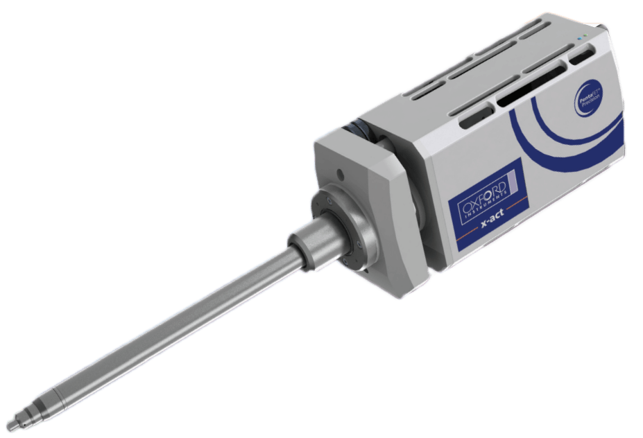
Energy-dispersive X-ray spectroscopy (EDS, EDX, or XEDS), sometimes called energy dispersive X-ray analysis (EDXA) or energy dispersive X-ray microanalysis (EDXMA), is an analytical technique used for the elemental analysis or chemical characterization of a sample. It relies on an interaction of some source of X-ray excitation and a sample. Its characterization capabilities are due in large part to the fundamental principle that each element has a unique atomic structure allowing unique set of peaks on its X-ray emission spectrum.
Appropriate for: 6th grade +
Available at: ECC

Field Emission Electron Probe Microanalyzer (FE-EPMA)
An electron microprobe (or electron probe microanalyzer) is a specialized scanning electron microscope, optimized for accurate and precise quantitative compositional analysis of solid materials at the micro-scale. It is fundametally the same as an SEM, with the added capability of chemical analysis. By using a field emission type electron gun, a smaller light source is possible and resolution is greatly improved. This makes it possible to analyze smaller microscopic areas. It is used for imaging of sample morphology and compositional variation, as well as compositional analysis by X-ray spectroscopy with ~1% precision.
Appropriate for: 8th grade +
Available at: Caltech
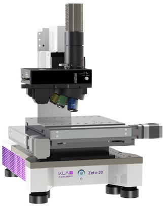
Optical Profiler
An optical profiler is a type of characterization equipment used for obtaining true color 3D data of a surface at the sub-micron level. Optical profilers combine key attributes of optical microscopes and standard stylus-type profilers. An optical profiler achieves the true color and wide field of view (FOV) nature of an optical microscope while simultaneously obtaining the nanometer level z-resolution of a standard stylus profiling technique.
Appropriate for: all grade levels
Available at: Rio Salado College
Scanning Electron Microscope (SEM)
A scanning electron microscope (SEM) is a type of electron microscope that produces images of a sample by scanning it with a focused beam of electrons. The electrons interact with atoms in the sample, producing various signals that can be detected and that contain information about the sample’s surface topography and composition. The electron beam is generally scanned in a raster scan pattern, and the beam’s position is combined with the detected signal to produce an image. SEM can achieve resolution better than 1 nanometer. Specimens can be observed in high vacuum, in low vacuum, in wet conditions (in environmental SEM), and at a wide range of cryogenic or elevated temperatures.
The Field Emission Scanning Electron Microscope (FESEM) has a much brighter electron source and smaller beam size than a typical SEM, increasing the useful magnification of observation and imaging up to 500,000x. The FESEM has enhanced observation of very fine surface features, electron beam sensitive materials, and non-conductive materials. It is ideal for imaging polymer materials and thin films.
Appropriate for: all grades
SEM Available at: ASU, COSINC, ECC, SLCC
FESEM Available at: Caltech, COSINC, CNEU
Transmission Electron Microscope (TEM)
A TEM collects images of samples by passing a beam of electrons through the sample. This allows users to resolve the internal structure of samples. To produce a standard TEM image, the electron beam must be able to penetrate the sample, with many electrons being transmitted through it. The difference between the numbers of transmitted and scattered electrons from individual areas in the specimen results in the contrast necessary to form a TEM image. The LVEM5 Desktop TEM has a maximum magnification of 700,000x. This microscope can perform in three functions modes: TEM, SEM, and Electron Diffraction. TEM mode makes it possible to image nanomaterials and thin sections. Electron diffraction provides structural characterization of crystalline materials.
Appropriate for: all grade levels
Available at: SLCC
back to top ↑
Limited Interaction / Mostly Demonstration
3D Nanoprinter (Lithography)
Nanoscribe’s 3D Microfabrication systems and solutions are based on Two-Photon Polymerization (2PP). 2PP is a key enabling technology for high-precision 3D printing objects and structures of virtually any shape with submicron details. Minimum XY feature size: 160 nm typical; Finest XY resolution: 400 nm typical.
Appropriate for: all grades
Available at: COSINC, GATech
X-Ray Fluorescence (XRF)
XRF is the emission of characteristic “secondary” (or fluorescent) X-rays from a material that has been excited by being bombarded with high-energy X-rays or gamma rays. The phenomenon is widely used for elemental analysis and chemical analysis, particularly in the investigation of metals, glass, ceramics and building materials, and for research in geochemistry, forensic science, archaeology and art objects such as paintings.
Appropriate for: all grade levels
Available at: NCMN/NNF University of Nebraska-Lincoln
back to top ↑
RAIN Partners
Arizona State University (ASU)
The Nanotechnology Collaborative Infrastructure (NCI-SW)
Tempe, AZ
https://ncisouthwest.org/
Tools:
• Phenom Pro Scanning Electron Microscope
Contacts:
Jessica Hauer
Faculty Associate
jessica.hauer@asu.edu
Rio Salado College
A Maricopa Community College
Tempe, AZ
https://www.riosalado.edu/
Tools:
• Zeta 20 Optical Profiler
Contacts:
Rick Vaughn
Faculty Chair – STEM Initiatives
rick.vaughn@riosalado.edu
California Institute of Technology (Caltech)
The Geological and Planetary Science Division’s Analytical Facility
Pasadena, CA
https://www.caltech.edu/
Tools:
• Field Emission Scanning Electron Microscope
• Field Emission Electron Probe Microanalyzer
• Micro-Raman Spectrometer
Contacts:
Chi Ma
Instrument Operator
chima@caltech.edu
626-395-6126
Paul Asimow
Principal Investigator
asimow@caltech.edu
626-395-4133
University of California San Diego (UCSD)
San Diego Nanotechnology Infrastructure (SDNI)
San Diego, CA
http://sdni.ucsd.edu/
Tools:
• Zeiss Sigma 500 Scanning Electron Microscope
Contacts:
Yves Theriault, PhD, PMP
Director, Education Programs and Outreach
ytheriault@ucsd.edu
858-210-0543
Colorado Shared Instrumentation in Nanofabrication and Characterization (COSINC)
University of Colorado Boulder
Boulder, CO
https://www.colorado.edu/facility/cosinc/
Tools:
• JEOL JSM-7401F Field Emission Scanning Electron Microscope
• Hitachi SU3500 VP Scanning Electron Microscope
• Nanosurf Drive Atomic Force Microscope
• Nanoscribe 3D Nanoprinter
Contacts:
Aju Jugessur
COSINC Director
aju.jugessur@colorado.edu
303-735-5019
Tomoko Borsa
COSINC-CHR Facility Manager/Scientist
borsa@colorado.edu
303-735-0203
Adrian Gestos
adrian.gestos@colorado.edu
Georgia Institute of Technology (GATech)
Institute for Electronics and Nanotechnology (IEN)
Atlanta, GA
https://www.sums.gatech.edu/articles/aboutus2
Tools:
• Zeta Sizer Nano ZS
• Olympus Confocal Microscope
• Fourier Transform Spectroscopy
• Nanoscribe 3D Lithography
• Exaddon Ceres Metal 3D Printer
Contacts:
Nikolas Roeske
nroeske3@gatech.edu
Grand Valley State University (GVSU)
School of Engineering
Grand Rapids, MI
https://www.gvsu.edu/engineering/
Tools:
• Agilent 5400 Atomic Force Microscope
Contacts:
Dr. Heidi Jiao
Program Chair of Electrical Engineering
Jiaoh@gvsu.edu
616-331-6844
Dr. Atilla Ozgur Cakmak
Assistant Professor of Electrical Engineering
cakmaka@gvsu.edu
616-331-6017
Normandale Community College
Vacuum and Thin Film Technology
Bloomington, MN
https://www.normandale.edu/academics/degrees-certificates/vacuum-and-thin-film-technology/index.html
Tools:
• Remotely Accessible Rough Vacuum Equipment Trainer (RA-RVET) System
• Remotely Accessible High Vacuum Equipment Trainer (RA-HVET) System
Contacts:
Nancy Louwagie
Instructor, Vacuum and Thin Film Technology
nancy.louwagie@normandale.edu
952-358-8738
NCMN/NNF University of Nebraska-Lincoln
Nebraska Center for Materials & Nanoscience
Nebrask Nanoscale Facility
Lincoln, NE
https://nanoscale.unl.edu/
Tools:
• X-Ray Fluorescence
Contacts:
Steve Wignall
NCMN Program Associate
swignall4@unl.edu
402-472-6078
Jodi Sangster
Nebraska EPSCoR- Instrumentation and Outreach
jodisangster@nebraska.edu
SUNY Erie Community College (ECC)
State University of New York
Williamsville, NY
https://www.ecc.edu/
Tools:
Remote Hands-on:
• JEOL JSM-6010LA Scanning Electron Microscope with Energy Dispersive Spectroscopy
• JEOL JSM-IT100 Scanning Electron Microscope
• Bruker – Dektak XTA Surface Profiler (motorized stage)
• Zeiss – Axio Imager D1.M Optical Microscope with motorized stage
Demonstration Only:
• Bruker – Multimode 8 Scanning Probe Microscope Atomic Form Microscope
• Gaertner Scientific – Stokes Ellipsometer LSE-USB
• Kurt J. Lesker – custom Vacuum System trainers
• OAI – Model 200 Contact Mask Aligner
• Kurt J. Lesker – ALD150LE Atomic Layer Deposition tool
• Lithography process
Contacts:
Rich Hill
hill@ecc.edu
716-851-1514
cell: 716-464-0136
Center for Nanotechnology Education and Utilization (CNEU)
Penn State University
State College, PA
https://cneu.psu.edu
Tools:
• Zeiss Field Emission Scanning Electron Microscope
• Atomic Force Microscope
• Cleanroom Tours
Contacts:
Trey Shirley
Lab Manager
tes5559@psu.edu
Renee Lindenberg
RAIN Coordinator
rll19@psu.edu
Salt Lake Community College
Microscope Lab
Salt Lake City, UT
https://www.slcc.edu/microscopy/index.aspx
Tools:
• Atomic Force Microscopes (CoreAFM, NanoSurf II, Portable Naio)
•Hitachi TM3000 and TM4000 Desktop Scanning Electron Microscopes
• LVEM5 Desktop Transmission Electron Microscope
• OMAX Optical Microscope
• Carbon Nanotube Furnace
• SU-8 Photolithography Station
Contacts:
Wesley Sanders
wesley.sanders@slcc.edu
801-957-3894
Micron-NSU Nanofabrication Cleanroom
Norfolk State University
Norfolk, VA
https://www.nsu.edu/cleanroom
Tools:
• Kurt J. Lesker PVD 75 Thermal Evaporator
• OAI 800 Mask Aligner
• Trion Phantom Reactive Ion Etch System
Contacts:
Hargsoon Yoon
hyoon@nsu.edu
back to top ↑
Additional Resources
Laboratory Guides
• Geology Mineral Lab (nanoHUB)
• Plant Growth in Solution of Nanoparticles (nanoHUB)
• Determination of Percent Oxygen in Air (nanoHUB)
• Gold Nanoparticle Synthesis and Characterization (nanoHUB)
• Nickel Nanowire Synthesis and Characterization (nanoHUB)
• Silver Nanowire Synthesis and Characterization (nanoHUB)
• Dye-Sensitized Nanocrystalline Solar Cell Fabrication and Characterization (nanoHUB)
• Mystery Molecules: Identifying Materials with Nanoscale Characterization Tools (NNCI)
• Seeing Nano I: Using scanning electron microscopy (SEM) to view nano-size objects (NNCI)
• Seeing Nano II: Using atomic force microscopy to view nano-size objects (NNCI)
• Silver nanoparticles synthesis, spectroscopy, and bacterial growth (NNCI)
• Synthesis and Characterization of CdSe Quantum Dots (NNCI)
• Synthesis and Stability of Silver Nanoparticles (NNCI)
Additional Videos
Introduction to Scanning Electron Microscope
Operation of CNEU (PSU) FESEM
Remote Operation of CNEU (PSU) AFM
back to top ↑


