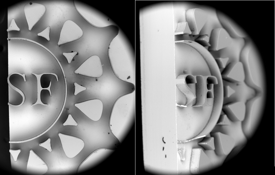
Here at the University of New Mexico’s MTTC Cleanroom, we have the ability to etch very deep, and very straight patterns into crystalline silicon wafers with the use of an Alcatel DRIE tool. This $750K machine consists of high vacuum chamber, water cooled systems, RF and LF generators and complex gas handling systems to provide a consistent well controlled “BOSCH” process. This plasma process utilizes sulfur hexafluoride (SF6) and octafluorocyclobutane (C4F8) gasses. By itself, SF6 plasma etching results in isotropic profiles – meaning the etch results in bowl shaped profiles – not straight! To overcome this, the etch process includes a passivation step meaning there needs to be something deposited to protect from the lateral etching – C4F8 is used; it forms a Teflon-like coating on the sides protecting the etched structure. By alternating between the two different gas flows every 5-10 seconds, one can etch very straight and deep structures, as shown in the accompanying figures.

Scanning electron microscope (SEM) image close up of the etch profile, note the scalloping pattern indicative of the cycling of etch and passivation steps. Etch ridge is about 400nm in depth. The view on the right shows the overall etch depth of about 100mm into the crystalline substrate. The desktop Phenom X at the University of New Mexico used is available as part of NACK’s RAIN network.


